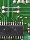
PANEL VOLTAGE AND TEST POINT
VON = VGH = VGON = VDDG = 20v to 30v
Gate-On Sales. VON good power supply for CKV_, CKVB_, and STVP high-voltage driver Results.
This VGH voltage (VGate High) is made up of DC-DC circuits. And their voltage is about 20V ~ 30V but it will depend on the construction of the T-con board. The VGH volume feature is offered to the Gate Driver Board as a “switch ON” feature.
VOFF = VGL = VGOFF = VEEG = -5v to -9v
Gate-Offers. VOFF is the power supply for CKV_, CKVB_, and STVP high-voltage driver outputs.
VGL (VGateLow) power is generated by the DC-DC phase as well. Some T-con boards will use a voltage as high as -15V or a low voltage as -1V. So it will depend on the design of the T-con and not much on the market. It is usually -5V ~ -7V. This undesirable voltage is provided by the Gate Driver Board. The VGL volume is similar to the “Turn Off” feature. When a VGL voltage supply is supply.
VDD = Vlogic = Vddd = Dvdd = 3.3v
Input Installation. VDD is the input driver of the scanner input.This VDD voltage comes from the DC-DC IC or uses an external Voltage Regulator IC to do so. 3.3V and other cables such as 2.5V (VDD25) and 1.8V (VDD18) using VDD 3.3V voltage converter. After the production of VDD power is fed into the Time Management section, the Source Driver Board and Gate Driver Board.
VDA = Avdd = Vdda = Vsource = 13v to 20v
This VDA voltage is approximately 14V ~ 20V and will depend on the design of their T-con board. VDA power is generated by DC-DC Converter circuits. It is used to donate to GAMMA circuits and access to the Source Driver Board
VCOM = 5.5v to 8.5v
half avdd suply use of pixel light output
STV = squre wave signal with a frequency of 92.72khz
Direct sync installation. The growing STV frontier starts the data framework. STVP input is used to produce high-resolution STVP output.
STVP
Extracting High-Voltage Scan-Drive. STVP is connected to VOFF when STV is low and connected to VON when STV is high and CPV1 is low. When both STV and CPV1 are high, STVP impedance is high
CPV1
CPV (Clock Pulse Vertical) -Vertical Clock Pulse Input. CPV1 controls the timing of the effects of CKV1 and CKVB1, which alters the status (by pre-charging sharing) at its falling ends.
CKV1
CKV (Clock Signal) - High-Voltage Scan-Drive output. When enabled, CKV1 switches between its higher state (connected to VON) and its lower state (connected to VOFF) on each falling edge of CPV1 input. In addition, CKV1 has a high impedance whenever CPV1 and STV are both low.
CKV2
Extracting High-Voltage Scan-Drive. When enabled, CKV2 converts between its higher state (connected to VON) and its lower state (connected to VOFF) on each falling edge of CPV2 input. In addition, CKV2 has a high impedance whenever CPV2 and STV are both low.


0 Comments